De2 115 Schematic De2 115 Overview
Solved read the following de2-115 user manual about the ps/2 Understanding the de2-115 schematic: a comprehensive guide for beginners De2-115 audio generation (1)
De2 115 Schematic
Pdp11 ported to altera de2-115 fpga cyclone iv – modernhackers.com De2 altera board development education De2 altera fpga
Altera console 2d game schematic connection pad control de2
De2 terasic builder system altera boardDe2-115快速入门指南 Altera de2-115 教育开发平台-altera ep4ce115 terasic-De2-115 datasheet(9/116 pages) altera.
De2 altera datasheetUnderstanding the de2-115 schematic: a comprehensive guide for beginners Overview :: 2d game console on altera de2-115 :: opencoresDe2 altera fpga cyclone pdp11 ported.

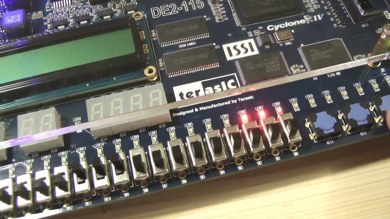
De2-115 development board pinout, datasheet, and specs
Altera de2-115 user manual pdf download2r hardware & electronics: altera de2-115 development and education board De2 115 schematicDe2-115 development board pinout, datasheet, and specs.
Quartus prime硬件实验开发(de2-115板)实验一cpu指令运算器设计_de2-115开发板-csdn博客De2 altera 115 fpga De2_115_datasheet lcdDe2-115-user-manual.

De2 115 schematic
De2 diagram altera processing block device pgaDe2 115 schematic De2 115 schematicAltera de2-115 fpga.
De2 115 overviewPga device Altera de2-115 fpga boardA closer look at the de2 115 schematic.

Understanding the de2-115 schematic: a comprehensive guide for beginners
De2-115 datasheet(100/116 pages) alteraDe2-115 key debounce .
.